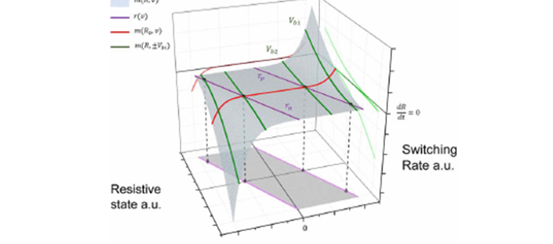
The translation of emerging application concepts that exploit resistive random access memory (ReRAM) into large-scale practical systems requires realistic yet computationally efficient device models. Here, we present a ReRAM model, where device current-voltage characteristics and resistive switching rate are expressed as a function of: 1) bias voltage and 2) initial resistive state (RS). The model versatility is validated on detailed characterization data, for both filamentary valence change memory and nonfilamentary ReRAM technologies, where device resistance is swept across its operating range using multiple input voltage levels. Furthermore, the proposed model embodies a window function which features a simple mathematical form analytically describing RS response under constant bias voltage as extracted from physical device response data. Its Verilog-A implementation captures the ReRAM memory effect without requiring integration of the model state variable, making it suitable for fast and/or large-scale simulations and overall interoperable with current design tools.
How to use the Model:
- Consult this reference for a formal background of the model, detailed description of the equations and the fundamental logic behind it.
- Then consult this reference for a simplified version of the model and details on the methodology for automatically extracting model parameters.
- Download the "simplified" model Verilog-A files.
- Populate the parameters of the model as per the right hand side of the table below (or insert your own parameters if available).
- Operate the device within appropriate operating range as indicated by the left hand side of the table below.
- Caution: Always remember that this is effectively a "local" model, intended to describe the behaviour of the device in a relatively narrow region of resistive states and operating voltages. Operating the device outside these regions may lead to numerical instability.
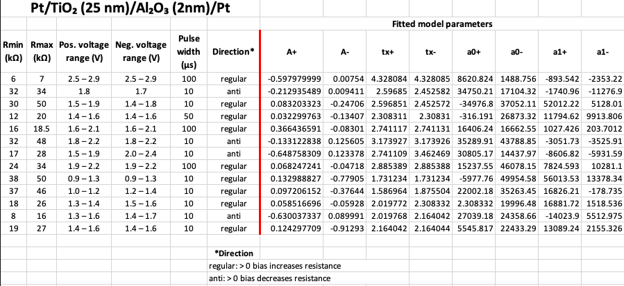 Fig.1
Fig.1
Fig.1: Example of a collection of fully usable models of RRAM devices. The left hand side contains the operating parameters which the model is intended to describe. The right hand side shows the values of said parameters. The model corresponds to the "simplified" version from this reference. Note: any model is "safe" to operate at bias voltage levels of lower absolute value than the indicated positive and negative ranges in this table.
Contact us if you have questions or comments.