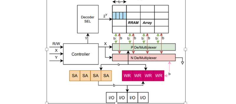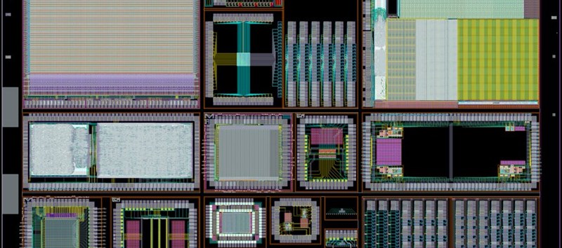
The purpose of the work is to give a holistic view of the memristor behavior from experimental analysis to its verification steps using a cadence virtuoso design environment. The work demonstrates with examples an end-to-end design flow for RRAM-based electronics, from the introduction of a custom RRAM model into our chosen CAD tool to performing layout-versus-schematic and post-layout checks including the RRAM device in a commercially available 180nm CMOS technology. The work is split into two parts. Part I presents an in-house fabricated Pt/TiOx/Pt VCM memristor model characterized and tested within the facilities at the University of Southampton which is followed by thorough step-by-step guidelines for integrating the model into the Cadence design environment for verification. Part II is more of a design and layout perspective showing by example the strategy to design CMOS circuits with memristors and a customized layout for the memristor cell. Also, instructions are provided for the standard cell to be integrated into the Calibre environment.
This step-by-step guide to introducing RRAM into the standard CMOS integrated circuit design flow is a useful reference document for both budding device developers who wish to benchmark their technologies and circuit designers who wish to experiment with RRAM-enhanced systems. In addition, the given design flow is versatile, robust and user-friendly as it can be adapted to different technologies, memristive models and other tool vendors, e.g. Synopsys, Tanner, and or modules e.g. Hspice, Assura, Pyxis, Eldo, etc.