Summary
Process maturity: Stable
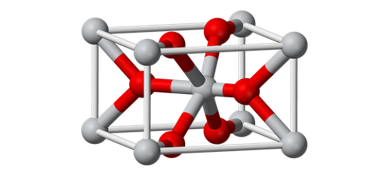
SnOx can behave as either n-type or p-type semiconductor depending on the defect type and density. It can be used for both RRAM and TFTs, therefore, it is a suitable material for CMOS integration and for all oxide 1T1R devices. The prepared SnOx-based RRAM devices show analog switching and either non-volatile or volatile behaviour depending on the electrode materials.
Active layer fabrication Data
|
Fabrication method: |
Magnetron sputtering |
|
Tool(s) used: |
Angstrom Engineering |
|
Main fabrication params: |
10 sccm of Ar flow, 20 sccm of O2 flow, 70 W power, 1 mTorr pressure |
|
Recipe |
Ar:O₂ |
Temp |
Comments |
|
Argon 10sccm, Argon 20sccm O2_10CP |
1:2 |
25°C |
XRD and XPS confirms SnO2 phase and pristine resistance is in few tens of MΩ range |
Electrode configuration
|
Top |
Bottom |
Tool |
Comments |
|
Pt (15 nm) |
Ti/Pt (10/15 nm) |
LAB700 |
Gradual change in resistance in pristine state, and Ohmic and SCLC mechanism when formed. |
Indicative data
|
Measurement: Pristine I-V characteristics (MΩ range resistance) Device stack: Ti/Pt/SnOx/Pt 10/15/30/15 (in nm, bottom to top) Active layer recipe: Argon 10sccmAr_20 sccm O2_10CP |
Measurement: I-V characteristics of a formed device (high resistivity TiOx; 4 nm AlOx) Device stack: Ti/Pt/SnOx/Pt 10/15/30/15 (in nm, bottom to top) Active layer recipe: Argon 10sccmAr_20 sccm O2_10CP Comments: Gradual resistive change, analogue behaviour and different mechanisms in set and reset |


